材料
III-V族光子学外延晶圆
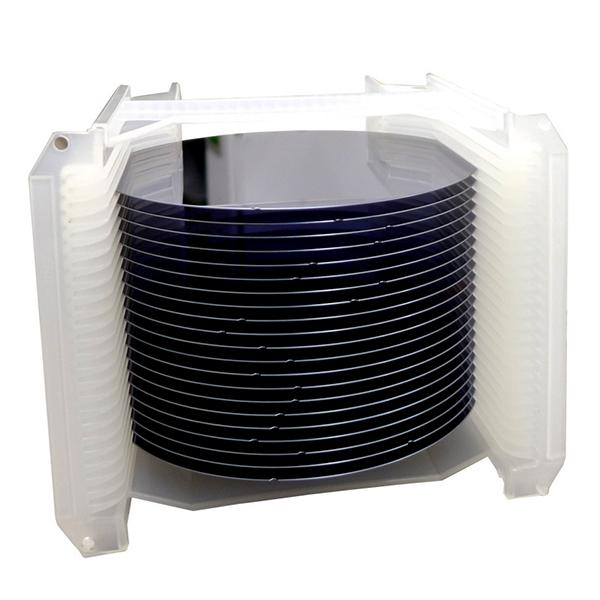
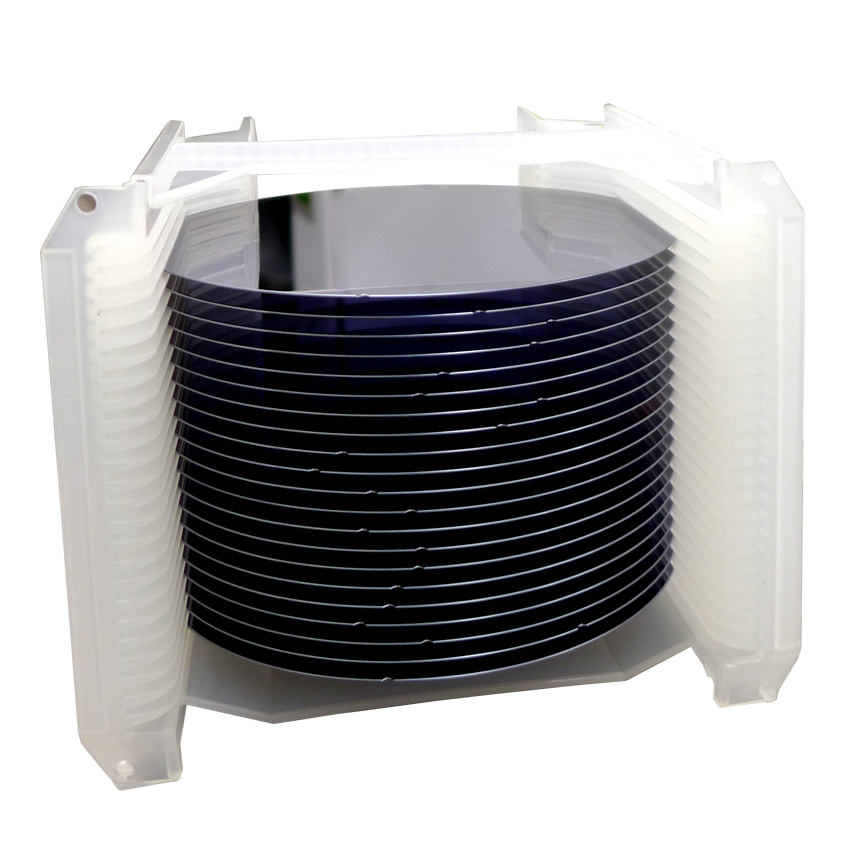
Deliver high-performance lasers, detectors, and other III-V semiconductor optoelectronic devices by fabricating with our consistent, high-quality epitaxial wafers.
The Coherent foundry employs a state-of-the-art MOCVD platform to deliver wafers which set a new standard for quality, performance, and yield. These meet the demands of challenging industrial, automotive, military, and communications applications.
III-V Photonics Wafer Capability
Source 2-inch to 6-inch wafers fabricated in our 25,000 square foot, Class 1000 cleanroom facility.
设备类型 |
基材 |
材料性能 |
晶圆直径 |
EpiLaser® (VCSEL, EEL, LED) |
砷化镓 |
AlGaAs/GaAs, InGaP/GaAs, InAlGaP |
最大150毫米 |
InP |
InP/InGaAs, InGaAsP, InAlAs, InAlGaAs |
最大100毫米 |
|
EpiDetector® (P-i-N, APD) |
砷化镓 |
砷化镓/砷化镓,磷化铟/砷化镓 |
最大150毫米 |
InP |
InP/InGaAs, InGaAsP, InAlGaAs |
最大100毫米 |
|
EpiSolar™ (1J, 2J, 3J, 4J) |
GaAs, Ge |
InGaP/GaAs/InGaAs, InAlGaP, AlGaAs |
最大150毫米 |
InP |
InP/InGaAs, InGaAsP, InAlAs, InAlGaAs |
最大100毫米 |
相关产品
精选博客
SiC Circuitry Makes EVs Better
高意 全球少数几家拥有完整、垂直整合的碳化硅(SiC)制造能力的公司之一。我们的生产范围涵盖碳化硅晶圆和外延工艺,直至功率器件和模块。此外,凭借我们生产碳化硅材料时无可比拟的质量高意 是唯一一家能够成功实现从当前标准晶圆直径150毫米向200毫米过渡的供应商。

精选成功案例
Laser Framework 在西门子的数字工厂中崭露头角
高意 开发支持 高意 Laser FrameWork ,助力西门子成功实施其ID Link制造计划。
